HSE в stm32f3discovery
Вс июл 30, 2023 17:10:22
Здравствуйте, уважаемые мурковчане!) Помогите новичку разобраться с HSE на отладочной плате stm32f3-discovery. Объясняю свой трехдневный затык.
Во время настройки системы тактирования я столкнулся с тем, что частота этого тактирования вообще не такая, какая должна по идее быть. После прочтения мануала от st, оказалось, что на упомянутой плате отсутствует кварцевый резонатор, подключенный к контроллеру, однако он есть на st-link, встроеном в плату и следует использовать именно его. Также я нашёл/покрутил пример кода от st, однако при включении соотв.опций ничего не поменялось. Почему/что я делаю не так?
Мой код:
P.S. Когда использовал хал, проблем с этим не было, все работало. Пробовал посмотреть, как сделал все куб, но как то слегка запутался. Помогите, пожалуйста! Заранее благодарю
Во время настройки системы тактирования я столкнулся с тем, что частота этого тактирования вообще не такая, какая должна по идее быть. После прочтения мануала от st, оказалось, что на упомянутой плате отсутствует кварцевый резонатор, подключенный к контроллеру, однако он есть на st-link, встроеном в плату и следует использовать именно его. Также я нашёл/покрутил пример кода от st, однако при включении соотв.опций ничего не поменялось. Почему/что я делаю не так?
Мой код:
- Код:
uint8_t RCC_Init(void) {
   /* Clear bits */
   RCC->CR |= (uint32_t)0x00000001;
     /* Reset CFGR register */
   RCC->CFGR &= 0xF87FC00C;
     /* Reset HSEON, CSSON and PLLON bits */
   RCC->CR &= (uint32_t)0xFEF6FFFF;
     /* Reset HSEBYP bit */
   RCC->CR &= (uint32_t)0xFFFBFFFF;
     /* Reset PLLSRC, PLLXTPRE, PLLMUL and USBPRE bits */
   RCC->CFGR &= (uint32_t)0xFF80FFFF;
     /* Reset PREDIV1[3:0] bits */
   RCC->CFGR2 &= (uint32_t)0xFFFFFFF0;
     /* Reset USARTSW[1:0], I2CSW and TIMs bits */
   RCC->CFGR3 &= (uint32_t)0xFF00FCCC;
     /* Disable all interrupts */
   RCC->CIR = 0x00000000;
   /* Using 8Mhz crystal */
   RCC->CR |= RCC_CR_HSEBYP | RCC_CR_HSEON;  /*Вот здесь вот, при установке bypass ничо не меняется, тактирование вообще не слушает меня; чисто визуально, по миганию светодиода частота раз в 15 меньше, чем должна быть. (По SysTick - точнo также) Код мигания самый тривиальный, задержка через цикл for, нет смысла сюда приводить. На счет mco ничего, увы, не могу сказать, я пока шкет и у меня осциллографа нету */
   /* Wait for crystal */
   uint16_t i = 0;
   while (!(RCC->CR & RCC_CR_HSERDY)){
      if (i == UINT16_MAX){
         return 1;
      }
      ++i;
   }
   /* Flash 48 <= HCLK <= 72 */
   FLASH->ACR |= FLASH_ACR_PRFTBE | FLASH_ACR_LATENCY_1й;
   /* PLL input = 8Mhz, output = 72Mhz    */
   RCC->CFGR |= RCC_CFGR_PLLSRC | RCC_CFGR_PLLMUL9;
   RCC->CR |= RCC_CR_PLLON;
   i = 0;
   /* Wait for PLL */
   while (!(RCC->CR & RCC_CR_PLLRDY)){
      if (i == UINT16_MAX){
         return 1;
      }
      ++i;
   }
   /* Divide PLL for APB1*/
   RCC->CFGR |= RCC_CFGR_PPRE1_DIV2;
   /* Switch on PLL */
   RCC->CFGR |= RCC_CFGR_SW_PLL;
   /* Wait for switching on PLL */
   i = 0;
   while (!(RCC->CFGR & RCC_CFGR_SWS_PLL)){
      if (i == UINT16_MAX){
         return 1;
      }
      ++i;
   }
   RCC->CR &= ~(RCC_CR_HSION);
   return 0;
}
P.S. Когда использовал хал, проблем с этим не было, все работало. Пробовал посмотреть, как сделал все куб, но как то слегка запутался. Помогите, пожалуйста! Заранее благодарю
Re: HSE в stm32f3discovery
Вс июл 30, 2023 23:40:22
оказалось, что на упомянутой плате отсутствует кварцевый резонатор, подключенный к контроллеру, однако он есть на st-link, встроеном в плату и следует использовать именно его.
Не знаю как вы собрались использовать кварцевый резонатор эмулятора, но контроллеры STM32 вполне успешно могут работать вообще без какого либо кварцевого резонатора. Ищите в мануале раздел про тактирование и изучайте.PS: Сильно сомневаюсь в возможности использовать для тактирования МК резонатор эмулятора. Хотя схему вашей платы не вижу в своём хрустальном шаре - посему утверждать не буду.
Re: HSE в stm32f3discovery
Пн июл 31, 2023 13:29:48
- Код:
 /* Clear bits */
   RCC->CR |= (uint32_t)0x00000001;
Вы тут пытаетесь сбросить весь регистр? Если да, то вместо этого в младшем бите устанавливается единица, а остальные не изменяются. Точно не перепутали "побитовое ИЛИ" ( | ) и "побитовое И" ( & )?
Re: HSE в stm32f3discovery
Пн июл 31, 2023 21:27:15
скорее не | и &, а |= и =
вот так действительно очистит все биты (доступные для записи) и установит в 1 самый младший, то есть, включит внутренний генератор HSI
Добавлено after 7 minutes 4 seconds:
внутренняя схема генератора рассчитана на непосредственное подключение кварцевого резонатора, а не использование его от какого-то st-link и совместно с ним.
Это же просто странно.
Другое дело, тактироваться от внешней частоты...
- Код:
 /* Clear bits */
   RCC->CR = (uint32_t)0x00000001;
вот так действительно очистит все биты (доступные для записи) и установит в 1 самый младший, то есть, включит внутренний генератор HSI
Добавлено after 7 minutes 4 seconds:
на упомянутой плате отсутствует кварцевый резонатор, подключенный к контроллеру, однако он есть на st-link, встроеном в плату и следует использовать именно его.
внутренняя схема генератора рассчитана на непосредственное подключение кварцевого резонатора, а не использование его от какого-то st-link и совместно с ним.
Это же просто странно.
Другое дело, тактироваться от внешней частоты...
Re: HSE в stm32f3discovery
Пн июл 31, 2023 21:54:52
Martian писал(а):Другое дело, тактироваться от внешней частоты...
Так фактически это же оно и есть. Приходит 8 МГц и приходит. А что источником является программатор, ну так бывает.
Re: HSE в stm32f3discovery
Пн июл 31, 2023 22:12:47
ну, тогда так и надо говорить, что тактирование внешней частотой. А не какое-то совместное использование кварца.
А есть ли оно там - jcxz уже сказал, что неизвестно.
Добавлено after 7 minutes 51 second:
да, есть. но надо убедиться в перемычках
схема здесь:
https://docs.rs-online.com/5192/0900766b814876f9.pdf
Добавлено after 54 seconds:
Установить внешний резонатор тож можно...
Добавлено after 4 minutes 25 seconds:
а вообще, оказывается, если посмотреть документацию на эту штуку, то там есть такое:
То есть, можно просто посмотреть
А есть ли оно там - jcxz уже сказал, что неизвестно.
Добавлено after 7 minutes 51 second:
да, есть. но надо убедиться в перемычках
схема здесь:
https://docs.rs-online.com/5192/0900766b814876f9.pdf
Добавлено after 54 seconds:
Установить внешний резонатор тож можно...
Добавлено after 4 minutes 25 seconds:
а вообще, оказывается, если посмотреть документацию на эту штуку, то там есть такое:
2.3 PLL_SOURCE_HSE_BYPASS
In this mode, the HSE is bypassed with an external clock (fixed at 8 MHz, coming from STLINK circuit). It is used to clock the PLL, and the PLL is used as the system clock source.
Some hardware modifications are necessary to bypass the HSE with the clock coming from the ST-LINK circuit.
For more details, refer to section "4.10 OSC clock" in "STM32F3 discovery kit User manual (UM1570)".
Note: PLL_SOURCE_HSE_BYPASS is the default clock configuration.
То есть, можно просто посмотреть
Re: HSE в stm32f3discovery
Пн июл 31, 2023 22:25:28
Т.н. HSE - это генератор. У него есть соответствующая аппаратура (усилитель и прочая), которая ПОДКЛЮЧАЕТСЯ к ногам по параметру HSEON.
Второе. Режим Byp означает, что используется прямое соединение и на специальный порт подается внешняя частота логичекого уровня.
Третье. При включении =генератора= HSE. Так еще раз, для особо непонятливых - не HSE, а генератора HSE, той самой аппаратуры, которая подключена к выводам для (кварцевого) резонатора. При включении начинается процесс раскачивания резонатора и через ощутимый интервал времени (указано в DS) генерация признается нормальной и выставляется соответствующий бит готовности. Программно надо сидеть и тупо ждать, когда генерация станет устойчивой. Для этого есть соответствующая строчка кода.
Теперь, пихают непойми что на ход внешней частоты (сигнал логический, АСЬ??), после этого ТС включает режим Byp (что вообще не понятно, т.к. Byp с синусом непоймичего работать не обязан) и HSEON (погдключение аппаратуры генератора). Понятное дело, что генератор внутри MCU от столь [гм] обращения наверняка свалится. Хорошо, смотрим код - ожидание RDY достигнуто, значит генератор как-то запустился. Хорошо! ... бы.
Наличие HSE_RDY позволяет переключить тактирование на него, что и делается. Но, STM32 имеет защиту от [вписывается], при отказе HSE он перейдет в странный режим, но продолжит работу. Всё это описано в RM. Итак, генератор HSE работает, но не всегда, т.к. на него вплавили странный сигнал. Т.е. HSE_RDY пропадает, что вызывает серьезный exception (отвал системной частоты процессора) и сваливание на тактирование HSI с делителем.
Что делать в этой ситуации? Прочитать раздел HSE в RM и исправить самостоятельно.
Re: HSE в stm32f3discovery
Пн июл 31, 2023 22:44:49
демонстрационный код и блок схема мк не предполагает иного включения внешнего тактирования, кроме как через HSEON. Если точнее:
RCC->CR |= (uint32_t)(RCC_CR_HSEON | RCC_CR_HSEBYP);
RCC->CR |= (uint32_t)(RCC_CR_HSEON | RCC_CR_HSEBYP);
Re: HSE в stm32f3discovery
Вт авг 01, 2023 00:42:00
...ничо не меняется,...
если я правильно понял
Вы 8МГц от внутреннего ген. меняете на 8МГц от f103 и хотите увидеть разницу?
для задержки исп. цикл for() - забудьте, для конкретных таймингов исп. апп. таймер. здесь Вам не avr.
... должно быть в 15 раз ...
Вы видели в какие asm инструкции компилятор превратил ваш цикл ? вероятно - нет, так откуда уверенность про "15 раз"
Последний раз редактировалось a797945 Вт авг 01, 2023 06:33:30, всего редактировалось 1 раз.
Re: HSE в stm32f3discovery
Вт авг 01, 2023 06:28:46
Вот настройка тактирования для F407. Думаю, что у F3 если не один в один, то очень похоже.
Спойлер
- Код:
int __low_level_init(void)
{
    __disable_irq();

    // Настройка FLASH
    FLASH -> ACR = \
        FLASH_ACR_PRFTEN    |
        FLASH_ACR_ICEN      |
        FLASH_ACR_DCEN      |
        FLASH_ACR_LATENCY_5WS;

    // Тактирование ----------
    // Включаем HSE = 8 MHz
    RCC -> CR = _VAL2FLD( RCC_CR_HSITRIM, 16 ) | RCC_CR_HSION | RCC_CR_HSEON;

    while( !( RCC -> CR & RCC_CR_HSERDY ) )
    {};

    // Задаём источники тактирования и прескалеры SYSCLK = 168 МГц  USB = 48 МГц
    RCC -> PLLCFGR = \
        RCC_PLLCFGR_PLLSRC_HSE              |
        _VAL2FLD( RCC_PLLCFGR_PLLQ, 7 )     |
        _VAL2FLD( RCC_PLLCFGR_PLLN, 336 )   |
        _VAL2FLD( RCC_PLLCFGR_PLLM , 8 )    |
        RCC_PLLCFGR_PLLP_div2;

    RCC -> CR = \
        _VAL2FLD( RCC_CR_HSITRIM, 16 )  |
        RCC_CR_HSION |
        RCC_CR_HSEON |
        RCC_CR_PLLON;   //Включаем PLL

    while( !( RCC -> CR & RCC_CR_PLLRDY ) )
    {};

    // Переключаемся на PLL с установленнными ранее прескалерами
    RCC -> CFGR = \
        RCC_CFGR_MCO2_HSE               |
        RCC_CFGR_MCO2PRE_div1           |
        RCC_CFGR_MCO1PRE_div1           |
        RCC_CFGR_I2SSRC_PLLI2S          |
        RCC_CFGR_MCO1_HSE               |
        _VAL2FLD( RCC_CFGR_RTCPRE, 8 )  |
        RCC_CFGR_PPRE2_DIV1             |
        RCC_CFGR_PPRE1_DIV2             |
        RCC_CFGR_HPRE_DIV1              |
        RCC_CFGR_SW_PLL;

    SystemCoreClock = 168'000'000;

    RCC-> CR = \
        _VAL2FLD( RCC_CR_HSITRIM, 16 )  |
        RCC_CR_HSEON                    |
        RCC_CR_PLLON;                       // Выключаем HSI

    #ifdef __DEBUG_SRAM__

      SYSCFG->MEMRMP = 3;  //0x20000000 -> 0x00000000

    #endif

  return( 1 );
}
Re: HSE в stm32f3discovery
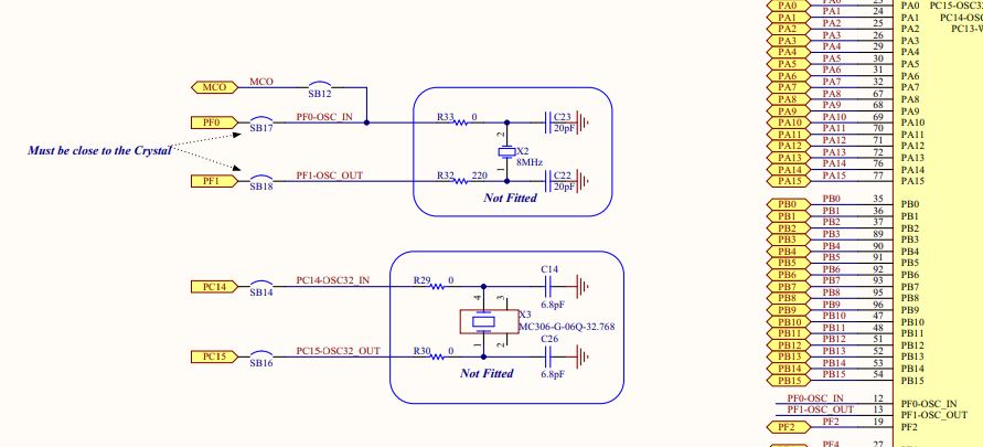
Вт авг 01, 2023 16:18:40
Большое спасибо всем, особенно, вам, Martian. Посмотрел user manual, всего то нужно было замкнуть SB12. Тем не менее, на счет некоторых мнений - вообще то, я опирался на код из примеров от st, где несколько товарищей углядели ошибки  . В доказательство приведу (форкнутый кем-то, кто ВОЗМОЖНО совершил ошибку) оригинал:
Может быть, конечно, я не прав, попробую разобраться
- Код:
void SystemInit(void)
{
  /* FPU settings ----------*/
  #if (__FPU_PRESENT == 1) && (__FPU_USED == 1)
    SCB->CPACR |= ((3UL << 10*2)|(3UL << 11*2));  /* set CP10 and CP11 Full Access */
  #endif

  /* Reset the RCC clock configuration to the default reset state ----------*/
  /* Set HSION bit */
  RCC->CR |= (uint32_t)0x00000001;

  /* Reset CFGR register */
  RCC->CFGR &= 0xF87FC00C;

  /* Reset HSEON, CSSON and PLLON bits */
  RCC->CR &= (uint32_t)0xFEF6FFFF;

  /* Reset HSEBYP bit */
  RCC->CR &= (uint32_t)0xFFFBFFFF;

  /* Reset PLLSRC, PLLXTPRE, PLLMUL and USBPRE bits */
  RCC->CFGR &= (uint32_t)0xFF80FFFF;

  /* Reset PREDIV1[3:0] bits */
  RCC->CFGR2 &= (uint32_t)0xFFFFFFF0;

  /* Reset USARTSW[1:0], I2CSW and TIMs bits */
  RCC->CFGR3 &= (uint32_t)0xFF00FCCC;

  /* Disable all interrupts */
  RCC->CIR = 0x00000000;

  /* Configure the System clock source, PLL Multiplier and Divider factors,
     AHB/APBx prescalers and Flash settings ----------*/
  SetSysClock();

#ifdef VECT_TAB_SRAM
  SCB->VTOR = SRAM_BASE | VECT_TAB_OFFSET; /* Vector Table Relocation in Internal SRAM. */
#else
  SCB->VTOR = FLASH_BASE | VECT_TAB_OFFSET; /* Vector Table Relocation in Internal FLASH. */
#endif
}
- Код:
static void SetSysClock(void)
{
  __IO uint32_t StartUpCounter = 0, HSEStatus = 0;

  /* SYSCLK, HCLK, PCLK2 and PCLK1 configuration ----------*/
#if defined (PLL_SOURCE_HSI)
  /* At this stage the HSI is already enabled */

  /* Enable Prefetch Buffer and set Flash Latency */
  FLASH->ACR = FLASH_ACR_PRFTBE | FLASH_ACR_LATENCY_1;

  /* HCLK = SYSCLK */
  RCC->CFGR |= (uint32_t)RCC_CFGR_HPRE_DIV1;

  /* PCLK = HCLK */
  RCC->CFGR |= (uint32_t)RCC_CFGR_PPRE1_DIV2 | (uint32_t)RCC_CFGR_PPRE2_DIV1;

  /* PLL configuration */
  RCC->CFGR &= (uint32_t)((uint32_t)~(RCC_CFGR_PLLSRC | RCC_CFGR_PLLXTPRE | RCC_CFGR_PLLMULL));
  RCC->CFGR |= (uint32_t)(RCC_CFGR_PLLSRC_HSI_Div2 | RCC_CFGR_PLLXTPRE_PREDIV1 | RCC_CFGR_PLLMULL16);

  /* Enable PLL */
  RCC->CR |= RCC_CR_PLLON;

  /* Wait till PLL is ready */
  while((RCC->CR & RCC_CR_PLLRDY) == 0)
  {
  }

  /* Select PLL as system clock source */
  RCC->CFGR &= (uint32_t)((uint32_t)~(RCC_CFGR_SW));
  RCC->CFGR |= (uint32_t)RCC_CFGR_SW_PLL;

  /* Wait till PLL is used as system clock source */
  while ((RCC->CFGR & (uint32_t)RCC_CFGR_SWS) != (uint32_t)RCC_CFGR_SWS_PLL)
  {
  }
#else
 #if defined (PLL_SOURCE_HSE)
  /* Enable HSE */
  RCC->CR |= ((uint32_t)RCC_CR_HSEON);
 #elif defined (PLL_SOURCE_HSE_BYPASS)
  /* HSE oscillator bypassed with external clock */
  RCC->CR |= (uint32_t)(RCC_CR_HSEON | RCC_CR_HSEBYP);
 #endif /* PLL_SOURCE_HSE */

  /* Wait till HSE is ready and if Time out is reached exit */
  do
  {
    HSEStatus = RCC->CR & RCC_CR_HSERDY;
    StartUpCounter++;
  } while((HSEStatus == 0) && (StartUpCounter != HSE_STARTUP_TIMEOUT));

  if ((RCC->CR & RCC_CR_HSERDY) != RESET)
  {
    HSEStatus = (uint32_t)0x01;
  }
  else
  {
    HSEStatus = (uint32_t)0x00;
  }

  if (HSEStatus == (uint32_t)0x01)
  {
    /* Enable Prefetch Buffer and set Flash Latency */
    FLASH->ACR = FLASH_ACR_PRFTBE | FLASH_ACR_LATENCY_1;

    /* HCLK = SYSCLK */
    RCC->CFGR |= (uint32_t)RCC_CFGR_HPRE_DIV1;

    /* PCLK2 = HCLK */
    RCC->CFGR |= (uint32_t)RCC_CFGR_PPRE2_DIV1;

    /* PCLK1 = HCLK */
    RCC->CFGR |= (uint32_t)RCC_CFGR_PPRE1_DIV2;


    /*  PLL configuration: PLLCLK = HSE * 9 = 72 MHz */
    RCC->CFGR &= (uint32_t)((uint32_t)~(RCC_CFGR_PLLSRC | RCC_CFGR_PLLXTPRE |
                                        RCC_CFGR_PLLMULL));
    RCC->CFGR |= (uint32_t)(RCC_CFGR_PLLSRC_PREDIV1 | RCC_CFGR_PLLMULL9);
    /* Enable PLL */
    RCC->CR |= RCC_CR_PLLON;

    /* Wait till PLL is ready */
    while((RCC->CR & RCC_CR_PLLRDY) == 0)
    {
    }

    /* Select PLL as system clock source */
    RCC->CFGR &= (uint32_t)((uint32_t)~(RCC_CFGR_SW));
    RCC->CFGR |= (uint32_t)RCC_CFGR_SW_PLL;

    /* Wait till PLL is used as system clock source */
    while ((RCC->CFGR & (uint32_t)RCC_CFGR_SWS) != (uint32_t)RCC_CFGR_SWS_PLL)
    {
    }
  }
  else
  { /* If HSE fails to start-up, the application will have wrong clock
         configuration. User can add here some code to deal with this error */
  }
#endif /* PLL_SOURCE_HSI */
}
Может быть, конечно, я не прав, попробую разобраться
Re: HSE в stm32f3discovery
Вт авг 01, 2023 19:06:30
Так фактически это же оно и есть. Приходит 8 МГц и приходит. А что источником является программатор, ну так бывает.
Внимательнее прочитайте что именно писал ТС в заглавном посте:на упомянутой плате отсутствует кварцевый резонатор, подключенный к контроллеру, однако он есть на st-link, встроеном в плату и следует использовать именно его.
Т.е. - использовать он хотел не логический выходной сигнал некоего генератора, а сам кварцевый резонатор. Что очень вряд-ли возможно. О чём я сразу и написал. Разве что если пожертвует тем ST-LINK-ом.